 Microchips – are indeed can be considered a black box – as long as it’s working you normally don’t look inside.
But what if you want to?
Today we’ll show how to “open” chips and what’s inside.
WARNING! All operations with concentrated (and especially hot) acids are extremely dangerous. Only trained persons should work with them using required protective equipment (acid-prof gloves, protection glasses, protective suit, fume hood and more). Remember that you only have 2 eyes!
This article is for educational purposes only, do not try to repeat!.
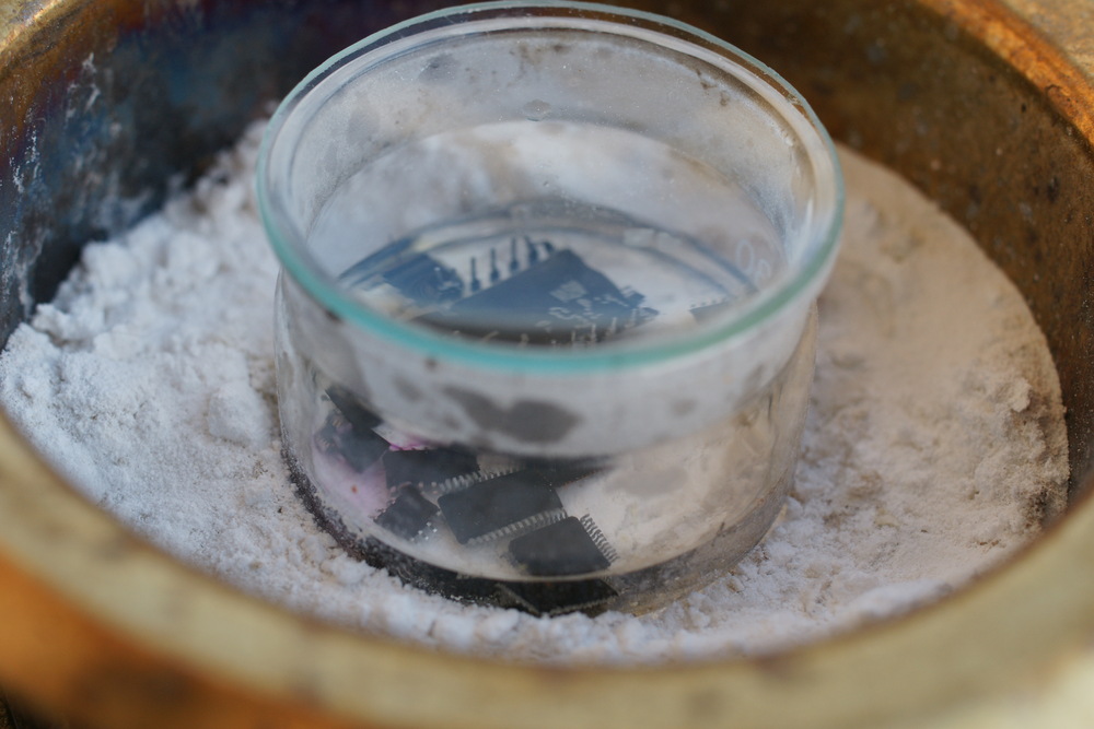
Take some microchips of interest and add concentrated sulfuric acid. Container should be closed, but not airtight, so that fumes can escape (that is extremely important). Heat it to boiling temperature (300 °C). White substance at the bottom is baking soda – it’s here to neutralize accidental spills and part of fumes.
After 30-40 minutes, acid “burns” plastic to carbon: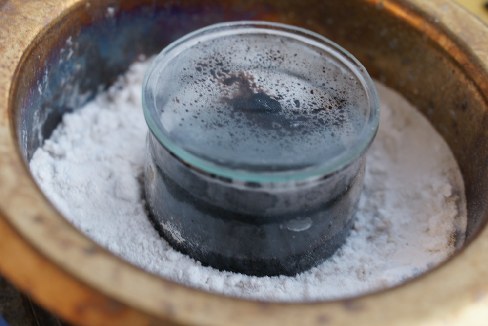
After it cools down, we can sort what is ready for next step and what needs another acid bath (thick, bulky packages usually need 2-3 rounds):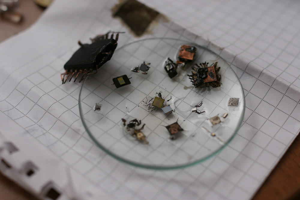
If pieces of carbon stuck to the microchip itself and cannot be removed mechanically, one can remove them in hot concentrated nitric acid (temperature is much lower, ~110-120 °C):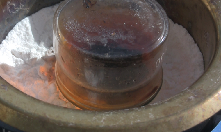
Images are clickable (beware of 5-25Mb JPEG’s).
Colors are enhanced, in reality they are much less saturated.
PL2303HX — USB<>RS232 converter, chips like this are used in Arduino-like boards for example: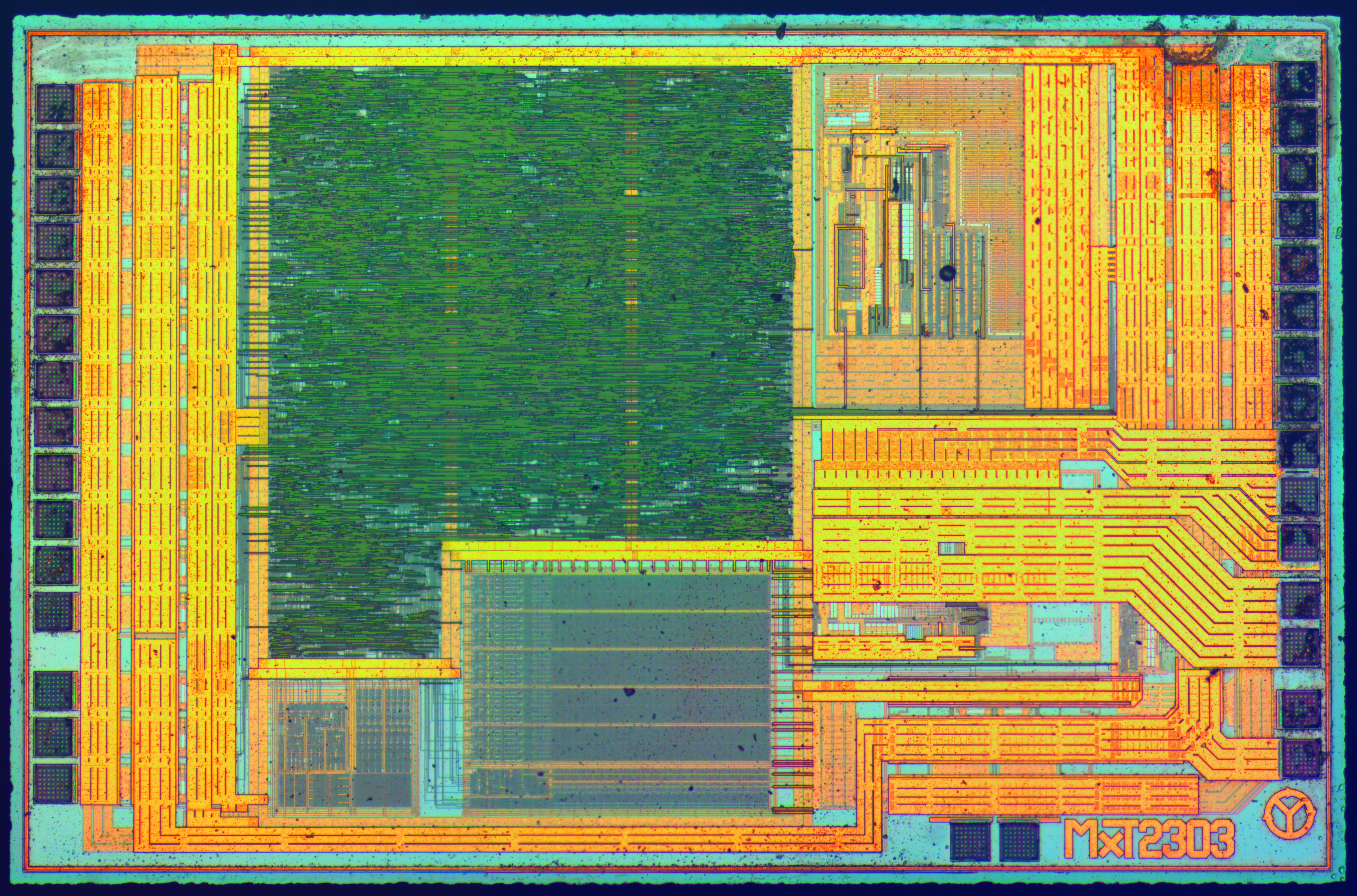
LM1117 — low-dropout linear regulator: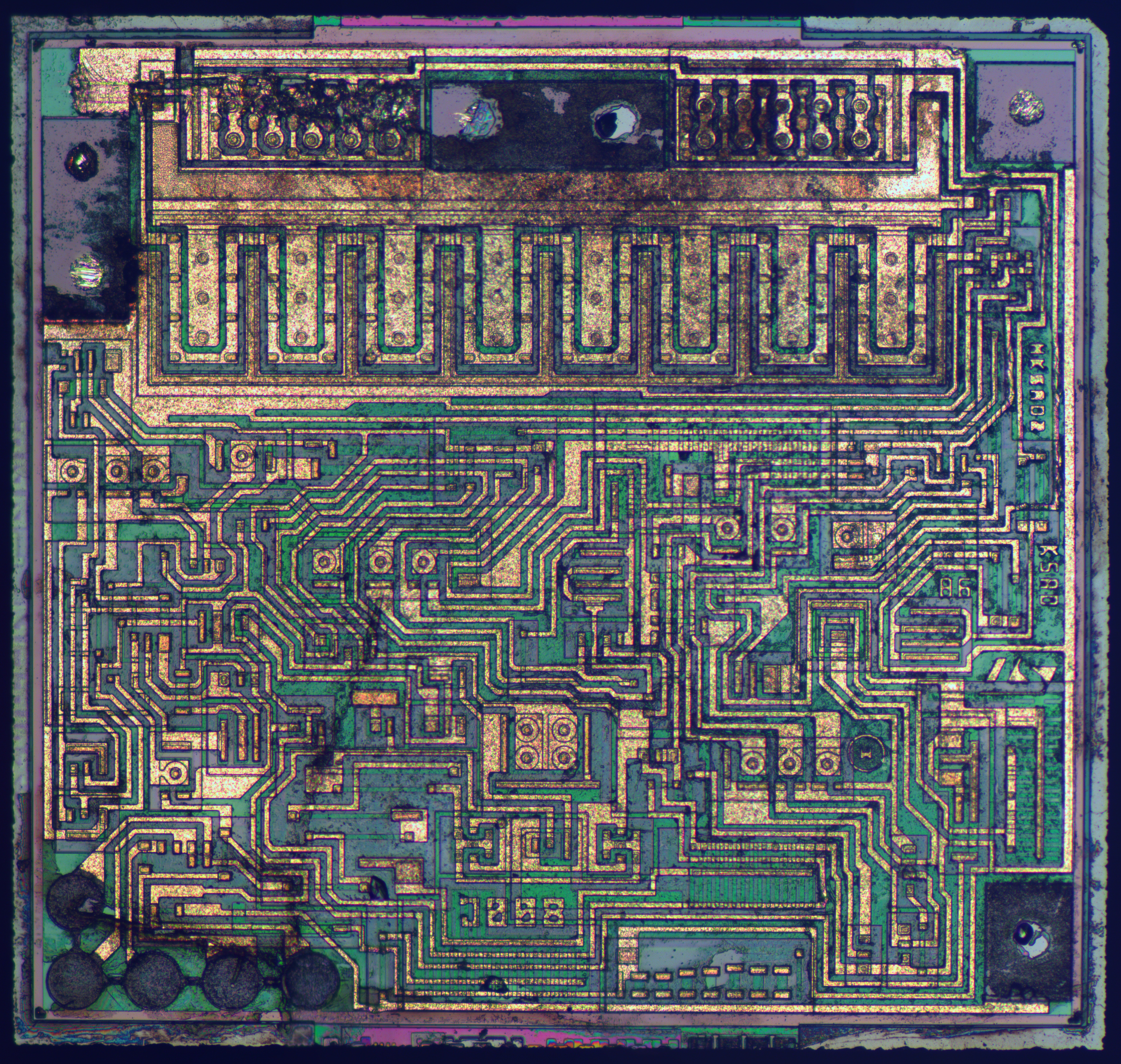
74HC595 — 8-bit shift register: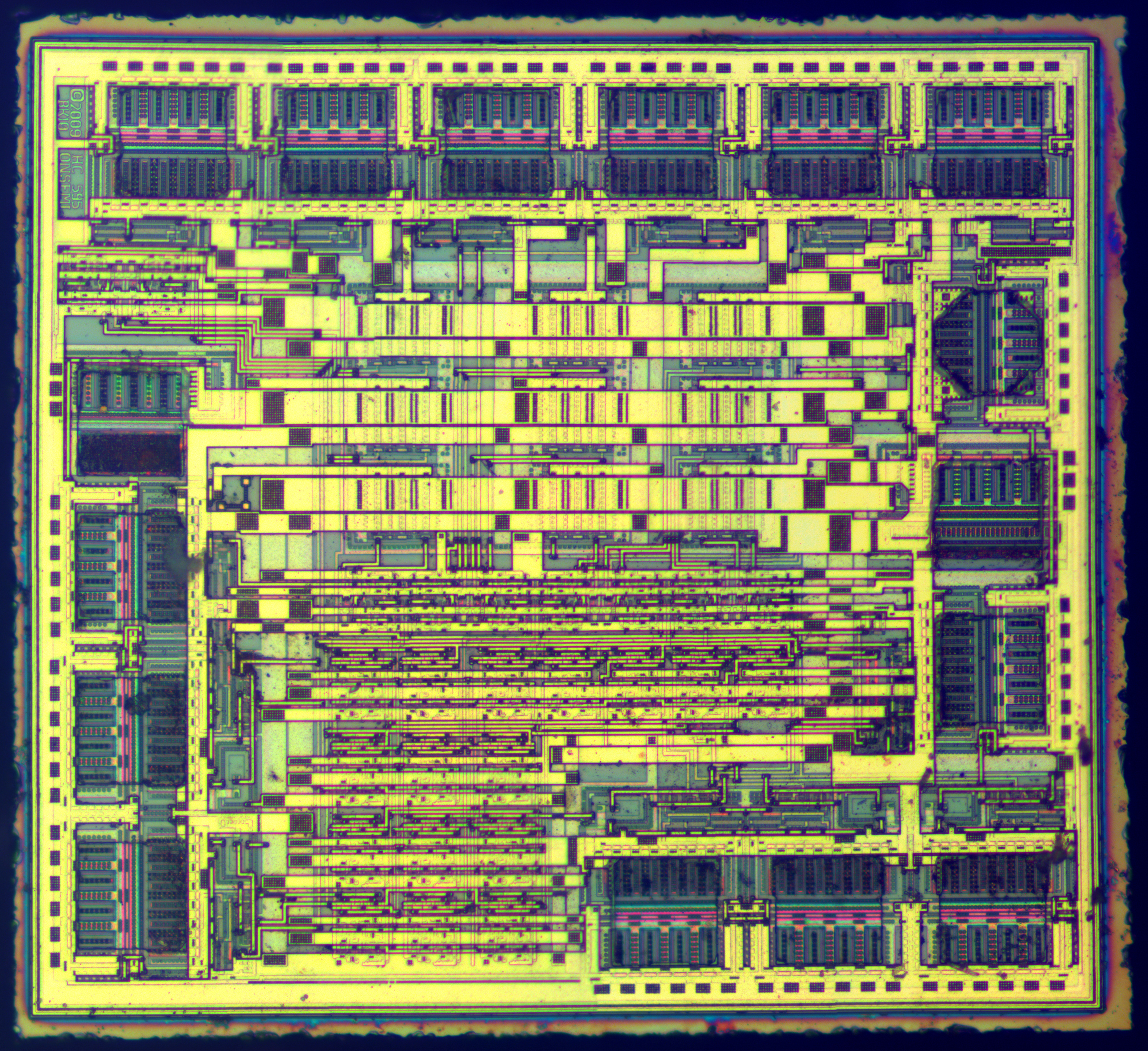
NXP 74AHC00 — quad 2-input NAND gate.
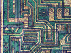
This is a nice example that ‘old’ tech nodes (1µm and older) are still in use. Also, note how many spare via are there for improved yield..
Micron MT4C1024 — 1 mebibit (220 bit) dynamic ram.
Widely used in 286 and 386-era computers, early 90’s.
Die size – 8662×3969µm.
AMD Palce16V8h GAL is an 32×64 array of AND elements.
GAL(Generic array logic) microchips are FPGA and CPLD grandfathers.
Die size – 2434×2079µm, 1µm technology.
ATtiny13A — one of the smallest Atmel’s microcontrollers: only 1kb of flash and 32 bytes of SRAM. Die size though appeared to be unexpectedly big (1620×1640 µm).
500nm technology node.
ATmega8 — one of the most popular 8-bit microcontrollers.
Die size – 2855×2795µm, technology node 500nm.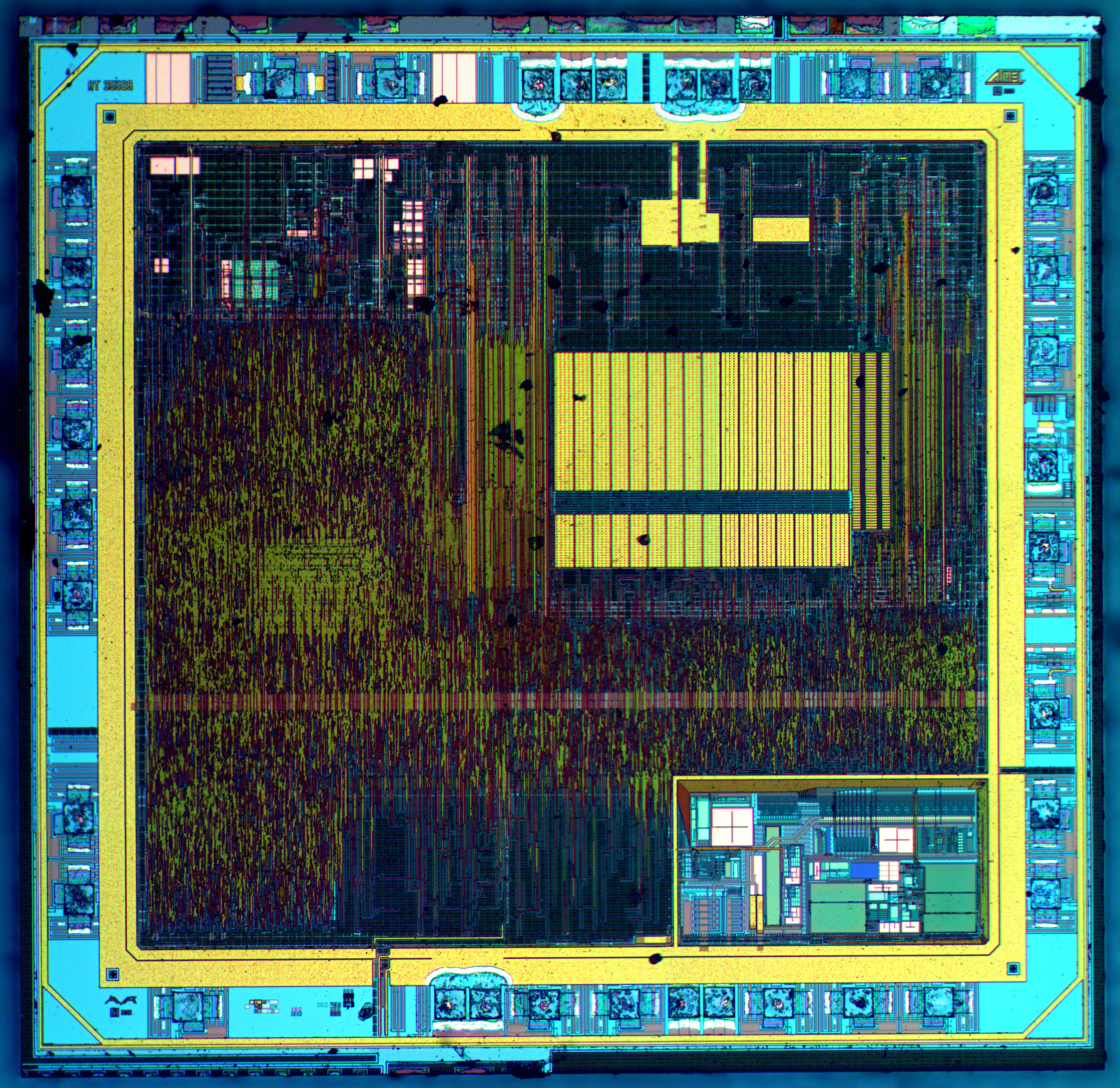
KR580IK80A (later renamed to KR580VM80A) – one of the most widespread soviet processors. Contrary to popular belief, it appeared to be not an Intel 8080A (or 8080) clone, but a code-compatible redesign (while several parts are quite similar, routing is different as well as pad placement).
Thinnest lines are 6µm. 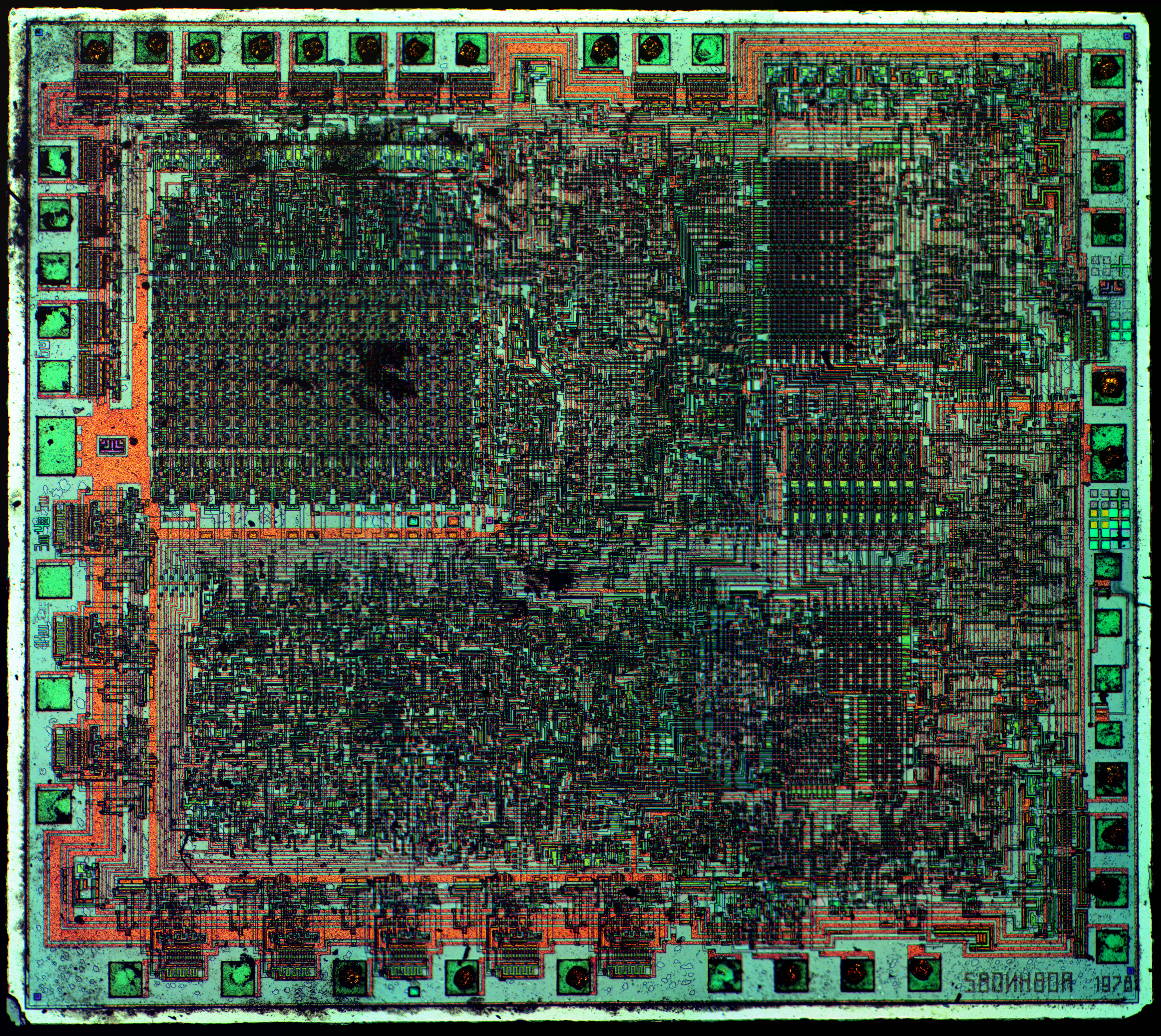
STM32F100C4T6B — is the smallest microcontroller made by STMicroelectronics based on ARM Cortex-M3 core.
Die size – 2854×3123µm.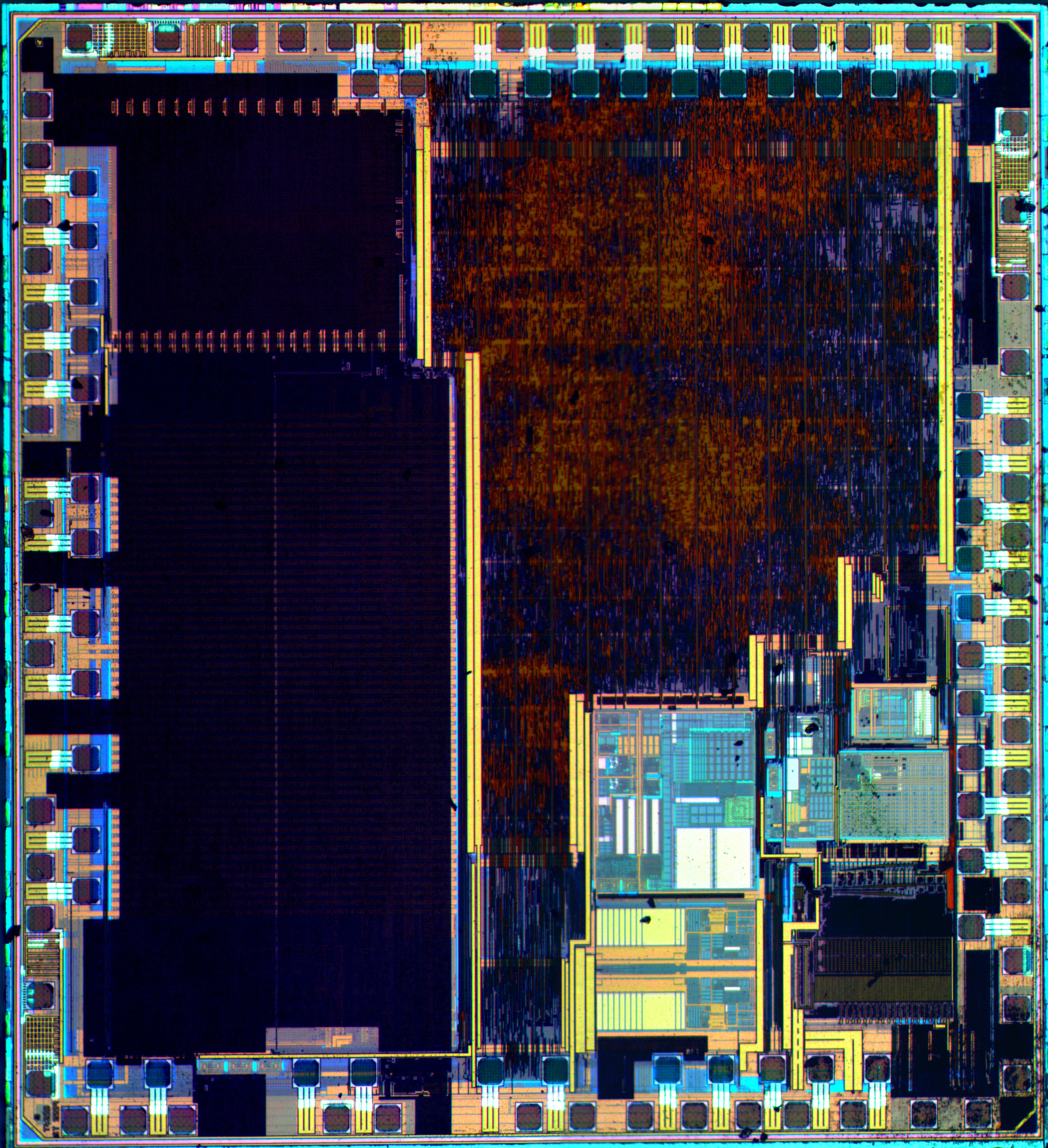
Altera EPM7032 — Altera EPM7032 – CPLD that have seen a lot… One of the last using 5V supply.
Die size – 3446×2252µm, technology node 1µm.
MIFARE chip, used in Moscow’s subway RFID tickets.
Die size – 640×620 µm.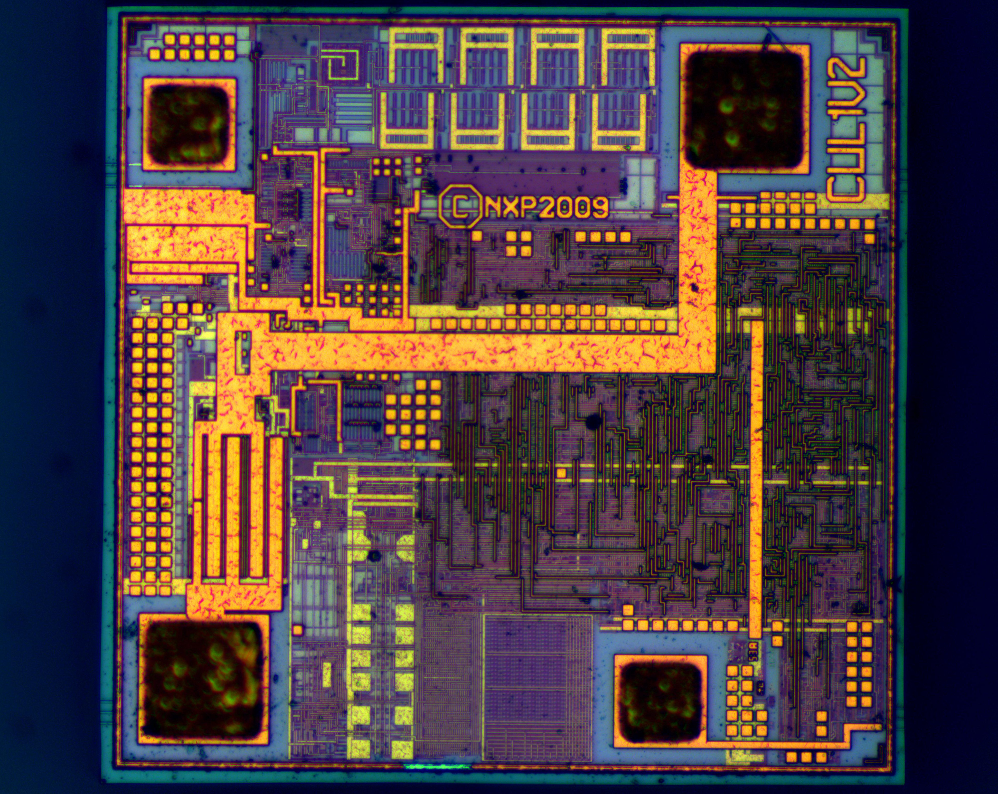
Now black box is open 🙂
Follow us on Twitter @Zeptobars or subscribe to our RSS feed – we’ll continue opening chips.
